Raspberry Pi 2 ARM-GPU IPC

Raspberry Pi 2 is powered by a Broadcom BCM2836 chipset. Along with the typical peripheral IP blocks like UART, SD, etc, BCM2836 ASIC integrates four ARM Cortex A7 cores and a graphics processing engine. The primary intent of this post is to elaborate the ARM – GPU inter-processor communication (IPC) mechanism. Essentially to explain the hardware and the software blocks involved in establishing a messaging channel between these two processors.

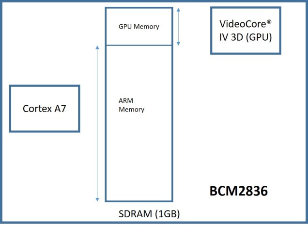
The basic infrastructure is illustrated by the diagram given below, we have the ARM processor and the VideoCore engine with a shared SDRAM. Note that the SDRAM would be an off chip module, so automatically there will be an external bus interface involved here. With these multiple processors and an SDRAM, the obvious IPC mechanism would be shared memory. But before getting into more details let’s have a brief overview of the RPi 2 boot.
System Overview
System Overview

Boot Process

BCM2836 boot binaries are located in the FAT formatted micro SD Card. Binaries for both GPU and ARM are in the FAT root directory. Once powered up, the very first boot step would be the execution of BCM2836 on-chip boot ROM, that would fetch second level bootloader which would in turn boot the GPU binary from SD. It’s GPU binary which is responsible for loading the ARM executable. More details about boot is can be read here, but for now we can crudely summarize the steps in the following manner.

  1. Power ON.
  2. BCM2836 BOOT ROM fetches second level bootloader.
  3. Second level boot loader fetches GPU binary.
  4. GPU binary loads the ARM image and transfers control.

So in this post we are looking to explain certain aspects of the ARM IPC code which is essential for communicating with the GPU. Please note that the second level bootloader and GPU binary images can be fetched from the GIT Hub repository. Now, let’s attempt to establish the fundamentals of this ARM-GPU IPC.

Shared Memory

To drive the graphics framebuffer or to accomplish any such task involving both ARM and GPU processing units, we require some meaningful message exchanges between these cores. For that we would use the shared SDRAM. But note that ARM-GPU combination is an asymmetric multiprocessing environment, so first we need to establish the processor level split for this 1G SDRAM. Basically this defines how much RAM is dedicated to each of these cores. This division is defined in “config.txt” configuration file located in the SDCARD, the relevant configuration parameter is mentioned below.

# GPU – CPU Split
gpu_mem=64

Note that “config.txt” is read by GPU during the boot process.

According to the documentation, the above “gpu_mem=64” setting should ideally allocate the top 64MB (address 0x3c000000 — 0x3FFFFFFF) of the SDRAM to GPU and the rest to ARM. But in reality this seems to be not the case, and the top 80MB is actually being taken by GPU and the bottom 944MB goes to ARM. Had to figure this out the hard way by messaging the GPU for its memory configuration, more on this later. Now the final high level split is illustrated below:

SDRAM Split
SDRAM Split


So now the binaries running on both ARM and GPU realize their own boundaries. Which is great, we cannot afford any form of cannibalism. Now we can introduce the next level of IPC synchronization — the Mailbox mechanism. This peripheral helps ARM and GPU communicate the exact location of the shared memory address where the larger shared message structures can be read or written.

Mailbox
Mailbox


The basic idea is simple; one Mailbox is for reading and the other for writing! Mailbox-0 read by Cortex A7 would be written by GPU, similarly GPU would read the Mailbox-1 which in turn would be written by A7. These 32-bit Mailbox registers are ideal for communicating that shared SDRAM memory address meant for ARM — GPU message exchanges.

Mailboxes

The four least significant bits (nibble) of the 32-bit address communicated through the message box is reserved for clarifying the Mailbox channel. This channel gives an indication of how to interpret the data structure at that transmitted address location. Note that each channel tends to have its own message structure, this implements a form of multiplexing over the same mailbox interface.

More details regarding these channels can be read here. Note that reserving the last 4 bits for channel number would also mean that the transmitted address has to be always aligned at 16 byte boundaries. But this seems more or less insignificant, because if the ARM Cortex A7 L1 cache is enabled, then to manage coherency we would anyway want buffers to be aligned at 64 byte cache line boundaries. Also, such shared buffers getting cached in L1 should be flushed before transmission and invalidated after it’s written by the GPU. Of course, all the shared memory address exchanges has to be physical bus address values, not virtual, otherwise they would make no sense.

Mailbox Register Encoding


An example of a 32-bit address transmitted over Mailbox channel 8 is illustrated above. Note that this encoding of the channel within the least significant nibble is a software mechanism. To the hardware these are mere 32bit values. Also, the channel number 8 which communicates property tags would be the one we use here for illustrating higher level data structures of the IPC. Now for some grisly register map details.


/* Register access helper */
#define REG(x)     (*(volatile unsigned int *)(x)) 

/* Mailbox 0 base address (Read by ARM) */
#define MBOX0_BASE 0x3F00B880

/* Mailbox 1 base address (Read by GPU) */
#define MBOX1_BASE 0x3F00B8A0

/* 
** Mailbox Controller Registers 
*/
/* I/O register is at the base address */
#define MBOX_RDWR(x)    REG((x))        

/* Status register at the offset 0x18 from base */
#define MBOX_STATUS(x)  REG((x) + 0x18) 

/* Status register value when mailbox is full/empty */
#define   MBOX_FULL     0x80000000      
#define   MBOX_EMPTY    0x40000000

/*  Interrupt configuration register */
#define MBOX_CONFIG(x)    REG((x) + 0x1C)

/* Configuration register mask to enable mailbox data IRQ */
#define   MBOX_DATAIRQEN  0x00000001 


For a successful mailbox transaction we only need the above three hardware registers and the associated bit masks.

  1. MBOX_RDWR : I/O register to transfer the 32-bit value
  2. MBOX_STATUS : Status register to synchronize the communication
  3. MBOX_CONFIG: Configuration register to enable interrupt generation

Below we have a write sequence transmitting a 32-bit value from ARM to GPU :


/* 1. Enable Mailbox0 interrupt to catch the GPU response,
this is optional if the read is going to happen in polled
mode. */
MBOX_CONFIG(MBOX0_BASE) |= MBOX_DATAIRQEN; 

/* 2. Before writing, loop until there is space
available in Mailbox1. This step may be optional
if the code always waits for a full transaction to complete. */
while (MBOX_STATUS(MBOX1_BASE) & MBOX_FULL);

/* 3. Write the 32 bit address into the Mailbox1 I/O register */
MBOX_RDWR(MBOX1_BASE) = ui32_address | channel;

Once ARM transmits the 32-bit value over Mailbox1, next step would be about waiting for a response on Mailbox0 written by GPU. Reading this 32 bit GPU response would mandate us to first wait for the interrupt and then read the MBOX_RDWR register.


/* 1. Now that the interrupt has fired, disable it. */
MBOX_CONFIG(MBOX0_BASE) &= ~MBOX_DATAIRQEN;

/* 2. Read the Mailbox 0 I/O register */
ui32_value = MBOX_RDWR(MBOX0_BASE);

Instead of interrupt, it’s also possible to poll on the Mailbox status register. Just wait looping for the bit MBOX_EMPTY to be reset.


/* 1. Poll the status */
while (MBOX_STATUS(MBOX0_BASE) & MBOX_EMPTY);

/* 2. Read the Mailbox 0 I/O register */
ui32_value = MBOX_RDWR(MBOX0_BASE);

Additionally we should also add the check to validate that the response is indeed for the expected channel.


do {
  /* 1. Poll the status */
  while (MBOX_STATUS(MBOX0_BASE) & MBOX_EMPTY);

  /* 2. Read the Mailbox 0 I/O register */
  ui32_value = MBOX_RDWR(MBOX0_BASE);
} while ((ui32_val & 0xF) != channel)

Now we have established a Mailbox based synchronization mechanism for both the cores to communicate shared memory addresses.

Data Structure

Mailbox merely enables the processors to transmit buffer pointers. The structure of this buffer contents would depend on the channel. Detailed specification of the shared memory data structures used for Mailbox channel 8 is linked here. Below we have a top level overview of that Channel 8 packet:


/* Packet HEADER */
struct header
{
  ui32 packet_length; // size in bytes (including header and values )

  /*
  ** Request codes:
  **        0x00000000: process request
  **        All other values reserved
  ** Response codes:
  **        0x80000000: request successful
  **        0x80000001: error parsing request buffer
  **                     (partial response)
  */
  ui32 req_resp_code;
};

/* Packet CONTENTS */
struct tags
{
  ui32 id; // id
  ui32 sz; // value size in bytes
  ui32 req_resp; // request/response code
  ui32 value[BUF_LEN]; // value length varies for each tag
};

/* Channel 8 Packet */
struct packet
{
  struct header pheader;
  struct tags ptags[NUMS];
};

Please note that the above illustration is to merely bring clarity to the high level structure of this packet. In reality it’s best to implement the packet generation using a ui32 array instead of the above structures.

The “struct packet” is essentially a header + sequence of tags, these tags are associated with a particular request like “Get VC memory” or “Get ARM memory”. In fact, these two tags were used to figure out the previously mentioned discrepancy of 64MB v/s 80MB in the ARM-GPU SDRAM split.

As mentioned in the link, these tag structures would be populated with requests by ARM, and GPU will overwrite them with responses. For example, “Allocate buffer” tag request would make GPU return a frame buffer address. After that, a valid frame written to this location will also get displayed on an attached HDMI monitor. We can even have multiple frames buffers and switch across them using “Set virtual offset” tag. Response time for this operation seems to be deterministic and around 300uS, which is good, otherwise we would end up having frame lags.


References:

  1. Linux Mailbox Driver
  2. Valvers : Graphics Basic
  3. GIT Hub GPU/Bootloader Repository
  4. Valvers : Bare Metal Programming in C Pt1
  5. Rpi2 config.txt documentation.
  6. Broadcom BCM2835 Peripheral Reference Manual
  7. Mailbox Property Interface 
  8. VideoCore® IV 3D Architecture Reference Guide
  9. BCM2835 Errata


DMA Architecture

DMA hardware is integral to most ARM SoC designs. They are extensively used for driving various peripheral controllers related to flash memory, LCD displays, USB, SD etc. Here we elaborate the functioning of a typical ARM SoC DMA controller and briefly delve into its internal mechanisms. The intent is to explain the underlying architecture of a typical DMA module and then eventually tie those elementary structural features to ARM’s PrimeCell® DMA Controller, which initially might come across as a more sophisticated hardware.

Direct memory access is simply meant to enable the processor to offload memory transfer operations. In this manner a system will be able to dedicate its valuable computational resources towards more apt alternate purposes. So, in fact we can state that a DMA controller is like a processor module which is capable of only executing load-store operations. While a full blown pipelined processor core possesses several other computational features and hence it should rarely be employed for rudimentary data transfers.

Eventually DMA is about transferring data across different hardware modules. Depending on the use case, the DMA source and destination might vary. And depending on the hardware the specifics of the bus protocol employed for load-store also varies. But just like a processor core, a DMA controller core will also be compatible with the hardware bus protocol features related to burst mode, flow control etc. Otherwise it simply won’t be able to move data around.


DMA-Processor-1
Fig 1 : DMA v/s Processor


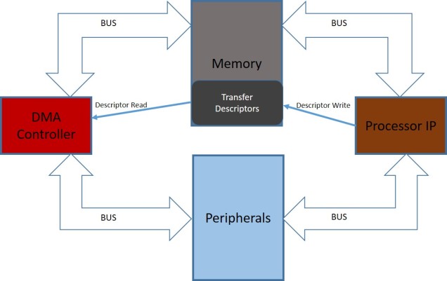
So, a DMA controller should be simply interpreted as a form of rudimentary logical block meant to implement data transfers. Similar to a processor core, this IP block also plugs into the larger data bus matrix involving SRAM and other peripherals. While a processor executes its object code from instruction memory, a DMA controller executes its operations by loading transfer configurations from a RAM memory segment. Such a configuration is usually termed as a descriptor. This recognizable structure would essentially describe all the details regarding the source/destination, burst size, length of the transfer etc. Eventually, such a configuration table would have to be loaded into the RAM by the DMA driver software running on the main processor. And usually the memory location of this descriptor table would be communicated to the DMA controller via some shared register.

Descriptor-2
Fig 2 : Descriptor

DMA controller is eventually a co-processor assisting the main core software with various complex use cases involving heavy data transfers. For example, populating an LCD image bitmap or transferring contents to an SD card are all DMA intensive features. Such a controller would usually support multiple DMA channels enabling simultaneous transfers. In this particular case, a DMA controller with more than two channels should be able to simultaneously drive an LCD and an SD Card.

An interrupt signal would be usually employed to synchronize these DMA transfers with the main processor operations. So, once the requested data transfer is completed, DMA hardware would simply assert an interrupt, which would be acknowledged by the processor.

DMA-int-3
Fig 3 : DMA Interrupt


Usually, the contents of a transfer descriptor would resemble the DMA controller register structures. Essentially, these memory descriptor contents are blindly loaded into its actual hardware registers by the DMA controller itself. For example, a descriptor would include entries for the source and destination address which would basically correspond to the actual DMA controller source and destination address registers. Such a DMA controller block would also involve a separate core logic which reads these registers and then implements the actual memory transfers. Illustrated by the Fig 4 below.

GenericDMA-4
Fig 4 : Generic DMA architecture

The transfer descriptor structures written to the memory by the processor would be loaded into the controller registers by the DMA hardware and eventually parsed and executed by its core load/store transfer logic. Undoubtedly, any errors within these memory resident transfer descriptors would also be propagated to the core transfer logic via these registers. Essentially, such a register set is meant to communicate all the relevant transfer configuration details to the DMA load/store engine. It clarifies all the details like source/destination, burst size, transfer length etc, but the actual circuit implementing the load-store loop would be already present within this DMA core.

Every hardware module has a primary interfacing mechanism, simple peripherals use registers and complex processors employ binary object codes. A typical DMA controller interfacing mechanism as elaborated above involves descriptor table reflecting its register set and transfer capabilities. PrimeCell is a DMA IP block from ARM, but unlike a typical DMA controller, its primary interfacing mechanism is not register set or descriptor tables. But it’s an instruction set, very much resembling a simple processor.

PrimeCell-5
Fig 5 : PrimeCell

PrimeCell integrates a rudimentary processor core which understands a limited instruction set, mostly meant for implementing load store operations and other synchronization mechanisms related to data bus and processor interrupts. So, here, instead of a descriptor table, we have an object code describing the transfer. Essentially a binary code implementing memcpy, but written using assembly instruction code understood by the PrimeCell DMA processor. Obviously, such an instruction code would also specify the source/destination address, burst size etc. It’s an actual binary object code.

PrimeCell6
Fig 6 : PrimeCell Architecture

This DMA processor core is also multi-threaded with one transfer channel being associated with each thread. These threads possess the same scheduling priority,  and the system implements a round-robin scheme. The internal FIFO is utilized as a buffer during DMA transfers and it’s shared across all the channels. Each channel is allowed access to the whole FIFO memory, but of course, at any instant, FIFO utilization across all the running channels can never exceed its total size. Such a flexible shared memory design adds to software complexity but it can also lead to a more productive hardware resource allocation pattern.

Finally, PrimeCell IP block also includes an instruction cache to optimize object code access. Also provides scope for instruction abort handling and watchdog exceptions to avoid lockups. In other words, the module almost resembles a full blown multi tasking processor. But do note that, such transfer related or hardware related exception triggers are present in a typical DMA controller also. So, seems like, with PrimeCell IP, a software engineer is being exposed to the underlying machinery which already exist in other typical DMA hardwares but is eventually hidden behind the veil of register set abstractions. As always, nothing is without a trade-off, the more complicated aspect of managing this module is definitely the object code generation. Which makes a crude compiler out of an otherwise relatively simple DMA driver.

SD Card Speed Class

All new SDCARDs conform to one of the speed classes defined by the specification, it’s usually stamped on top of the card and they are quite relevant for multiple reasons.

  1. It defines the speed at which you can clock the card, 50MHz for class 10 and otherwise 25MHz.
  2. Also alludes to the RU size, higher class cards pack more internal buffering.
  3. Finally its primary purpose is of conveying the maximum write speed, class 10 being the fastest.


SD Bus Clock

High clocking capability means better internal circuit and more the bill of material$, class 10 cards are said to be capable of high speed (50MHz) mode, at least that is what the spec claims but the scriptures may not always reflect the reality. Running an intensive I/O test showed that in practice even a 44MHz clock tends to choke most of the cards, actually two out of the four popular makes exhibited inconsistencies. Even though card’s CSD register mentioned 50MHz, the general card behavior tends to be intolerant to intensive use cases at higher clocks, sometimes even before switching to high speed mode (via CMD6) the CSD register claim 50MHz compliance which seems contrary to the spec and when practiced bricks or crashes the card. The root cause of the high speed non-compliance is not clear to me but the fact that certain cards are more tolerant than the others should be kept in mind while testing the system.

Buffering

Internal SDCARD buffers expedite I/O by implementing a producer-consumer like scenario, Class 4 cards tend to have an internal buffer (RU) size of 32K while for class 6 it goes up to 64K and for Class 10 a whopping 512K, not surprising that the price of the card also follows a similar pattern, runs from $5 to $10 & to around $30 for high speed cards. Optimal use of cards would be to write in terms of the RU sizes so that the card buffers are utilized to the maximum, writing more than the RU size will make the host unnecessarily wait for the card to flush data to internal flash and transmitting very small packets will only keep the SDCARD firmware unusually idle. Performance depends on the depth and also on the maximum utilization of available computational units within the pipeline. So, with regards to SDCARD also, we need to simultaneously engage the host and the card which eventually leads to better throughput.

Write Speed

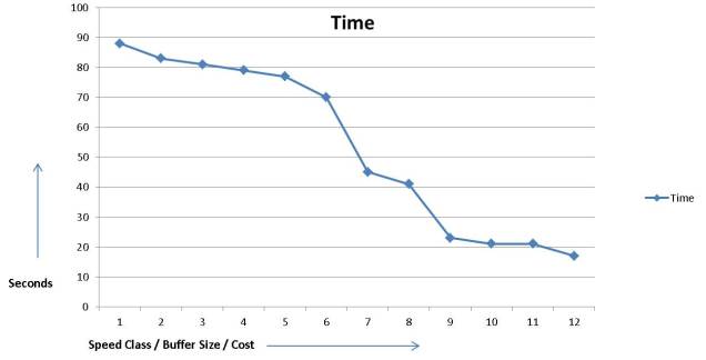
Time taken to write 128 MB of data was sampled over a dozen cards, Class 10 PNY card was the fastest at 17 secs while the slowest was 88 secs for the Transcend class 4 card. Below we have a graph which shows how the time to write is inversely proportional to the cost and the RU size and the speed class of SDCARDs. Embedded host used for this exercise was an Embedded  Artist EA 3250 board and it runs a 266MHz NXP controller.

Speed Class Time
Speed Class Time


Inference

Accurate class differentiation emphasized by the spec gets a tad obscured when it trickle down into the eventual product which seems to vary in behavior and performance capabilities across and within the same class. The challenge with SDCARD host productization is primarily that of interoperability testing, here we have considered only a dozen makes which is popular in the US, undoubtedly once we account for the China market there will be little semblance of sanity left in the above graph.

More on this topic – An account on SDCARD internals.

SD Card Flash Translation Layer

SD CARD protocol itself provides a rough blueprint of the internal design, but sometimes you can implement particular use cases hinging on the hints provided by the spec to expose certain limitations and strengths of the card machinery.  It’s well-known that an SD CARD runs on flash, usually a NAND MLC or an SLC but superficially it behaves nothing like a flash and the user need not fret about block erases, bit flips or wear leveling. All the complexities of a flash seemingly abstracted inside a black box, but we could still attempt to unearth certain aspects of this chaos.

Boot Code

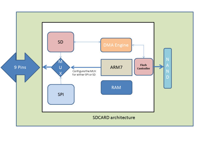
Once we supply the voltage, card internally figures out whether it’s being used with SPI or SD bus by sampling the card detect pin (pin 1), which is pulled high only for SD mode. Protocol implemented for these interfaces differ significantly, so their software stacks also differ and of course there also exist a small micro-controller driving this SD firmware.

The boot code checks pin 1, identifies the interface and jumps to the corresponding software interface stack, now lets consider that the card is connected over SD bus. The boot code ensures that the voltage supplied by the host is appropriate by using CMD8 & ACMD41, this boot process is driven by the host and we can imagine that the card start-up is completed only when the software enters what the spec defines as the transfer state.

The hardware pins are shared across both the modes, so there has to be an internal multiplexer which will configure the controller to drive the pins either with SD or with the SPI physical layer protocol. We can imagine that the chip set used will include the corresponding hardware IPs or at least some form of software implementation of the SD, SPI & multiplexer logic.

Transfer Mode

Boot up is completed once we enter the transfer mode, here the SD state machine is primarily meant to service I/O requests like sector reads, writes and erases. A DMA engine is most probably utilized for ensuring that the internal flash transfers happen in parallel with the SD I/Os, in other words the card might be transferring NAND pages to the flash while its receiving more data from the host via the SD interface. The read and write operations are pipe-lined and buffered to ensure the maximum throughput, especially for higher grade class 10 cards.

Image

Translation Layer

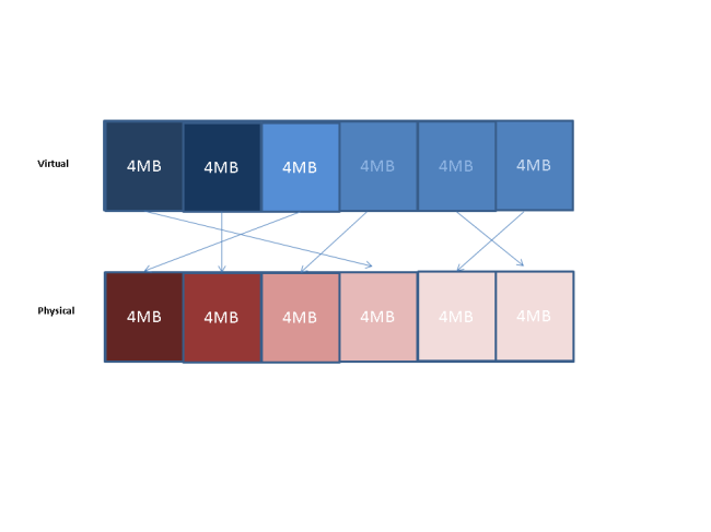
Flash contents cannot be over-written without intermediate erases. So, for any SDCARD I/O operation there exist a ‘translation’ from virtual to physical address. For example, lets consider that we wrote to the sector 1024 on the SDCARD, and this address got initially mapped to physical sector 1024 itself on flash. Later we overwrite the contents, but this time write cannot go to the same physical address because it needs to be erased before programmed again. Now the translation layer will have to remap the virtual address 1024 to another erased and clean physical address, say 2048. So, now the virtual sector 1024 translates to a different physical address. Similarly, every write to virtual address gets mapped to a physical address and every subsequent read of the location is translated to the very same address. These mappings are stored separately by the firmware and this way a translation layer will abstract the flash complexities from the card user who remains oblivious to the actual physical address locations. Obviously, the erase of dirty pages need to happen before they can be reused.

Every translation layer also requires a size for its maps, spec confirms that a card complying with speed class specification (class 2, 4, 6 & 10) will implement internal map size equal to its ‘Allocation Unit” (AU)  size, this can be read from one of the card registers. This means that the virtual to physical maps will be of AU size, which is typically 4MB.

Translation Layer Mapping


Flash Translation Layer Algorithm

Reads are straightforward, all SDCARD needs to do is access its mapping information and read the corresponding physical AU. Writes can be tricky depending on the use case, lets consider two types.

a. Contiguous writes
Writes are sequential — and cross AU boundaries only after the previous physical AU was completely written. Here the card translation layer will select a fully erased physical AU for the write and then flush the contents continuously. After each AU write, the older physical AU is marked dirty and queued for an erase, while the translation is remapped to the newly written AU. An illustration is given below.

Consider virtual AU 10 was mapped to physical AU 30 (PAU 30) before write, and when the IO starts the map algorithm selects (Physical) AU40 as the new physical map for virtual AU10 (VAU 10).

Sequential Write -- Initial State
Sequential Write — Initial State

Write starts at PAU40. After 4MB write ends, the VAU 10 presently mapped to PAU 30 gets remapped to PAU 40.

Sequential Write Done

PAU 30 is marked as dirty and added to the erase queue.

Quite easily the most simple and the fastest use case.

b. Random writes across AUs
Here we write at block addressed which are located at different AUs, quite similar to the use case where the FAT table and directory entry contents need to be updated in between a file write. Consider the following illustration:

Step one: 1MB write of file contents to VAU 10.
Step two: 512 byte FAT table write to VAU 1.
&
Step three: 512 byte directory entry write to VAU 8.

The first step will write 1 MB at VAU10 and then the file system moves on to write the FAT table located on VAU1, consider that before being written the VAU10 was previously fully used and contained 3MB of valid and 1MB of dirty data (3 + 1 = 4MB).

The steps executed inside the FTL with regards to the above file system operations are illustrated below.

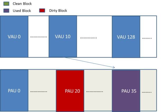
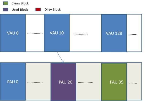
File clusters inside VAU10 was initially mapped to PAU20, when the write started a fully erased PAU 35 was selected as the new map (writes cannot happen on dirty flash blocks!).

Random Write -- Initial State
Random Write — Initial State

1MB of file contents were written to PAU35. Now 3MB of VAU 10 contents reside in PAU 20 and rest of the newly written 1MB is in PAU35.

Random Write -- Intermediate State
Random Write — Intermediate State

One VAU cannot be mapped to two physical AUs, so we have two options:
a. Either move the 3MB contents from PAU20 to PAU35 and then remap VAU10 to PAU35.

Random Write Final State

or
b. Do a partial erase of PAU 20 and move the new 1 MB from PAU35 to that location and maintain the same old map.

Random Write -- Final State
Random Write — Final State

SDCARDs might be using either one of the above two options, in the first case map information will be updated (VAU10->PAU20 modified to VAU10->PAU35) while the second case maintains the same map (VAU10 -> PAU20). Both the cases incur an overhead and this weighs heavily on the SDCARD write performance.

The above details alludes to the fact that an SDCARD tends to select an AU to which we write as the “active one”, so any writes to this ‘Active AU’ will have minimal overhead but as soon as we switch the write location outside of this ‘Active AU’ the map maintenance kicks in — essentially the garbage collection. Some of the class 10 cards can accommodate two active AUs and hence the overhead happens only during the above Step Three of the FAT file system write illustration given above, while the switch to the Step Two happens without a glitch.

Y-Axis: Time in uSecs, X-Axis : Write Count

Above graph illustrates the write times for the following three use cases:

1. Interleaved writes switch across VAUs continuously, first 4K bytes are written to an address on VAU1, second 4K to an address on VAU2 and so on.
2. Random writes switch VAUs for every fifth write, so 4K writes happen to four locations within VAU1 before it moves to VAU2 and so on. Here the number of times we switch VAUs are less that the first case.
3. Streaming 4K write is contiguous, AU switch happens only after the previous one is completely written, so there is no merge overhead and the number of times we switch AUs are least here.

Block Associative Sector Translation

Locality of reference is integral for achieving optimal write throughput. Quite visible from the graph that writes are faster when its contiguous, while its far from optimal when they are done across AU boundaries. Most probably SD CARDs should be employing a variant of block associative sector translation.

More on this topic – SDCARD Speed Class

In NAND memory, why is there a limit to the times we can make a partial write to a page?

A question posted on Quora — “In NAND memory, why is there a limit to the times we can make a partial write to a page? Is it because of write disturb. If so how does it happen? Does the same apply to partial reads?”

Having worked for some time on SLC NANDs, few points which comes to my mind are :

NAND data sheets from Samsung, Toshiba & Micron tend to limit the number of times a page can be partially programmed (usually to 4), this may be a circuit design decision which might have aided in some optimization with cost/speed/reliability etc. The exact reason could be only given by the NAND chipset designers.

Did observe that if we try, then we could partially program pages for more than the actually mentioned 4 times. But reliability is a question here! Four cycles of partial programming is a good number, if your software is doing frequent partial writes then it is inviting a performance hit.

Read disturbances are known to cause bit flips and excessive number of block erase cycles can lead to bad blocks. Not aware of any “write disturb”on SLCs.

NAND page read protocol will always fetch the data from the cells into an internal NAND chip RAM buffer from there the data can be sampled though any multi pin interface. In that sense, have not come across any hardware which allows partial read of physical NAND pages. We can definitely do random partial reads on a page after it is fetched from the NAND cells into this internal NAND chip buffer, but then this can be executed unlimited number of times

NAND flash musings

Been quite some time since the last post, life has been busy, thanks to the NAND flash chips from Toshiba & Samsung. Ironic enough their seemingly naive data sheets introduce NAND as an angelic technology. Simple protocols, even more simple hardware interface. A totally reasonable requirement  placed on driver to fix one bit errors and detect two bit errors (which is not supposed to happen but still for some unknown reason vendors mention this requirement too, would be ecstatic to know why). A touch of complexity is felt only when bad blocks are encountered, which is totally fair considering the cost effectiveness of NANDs.


My initial impression of NAND being a fairly simple fixed hassle free storage media was progressively crushed to shreds during the last one year of NAND torments. Have worked only on SLC NANDs from Toshiba & Samsung, they are extensively used on mobile handset platforms. So, MLC is an unknown inferno to me.  Hopefully the below mentioned points might help the posterity from enduring the crisis. Always remember to religiously follow the Data sheet (henceforth referred to as “the book”)  for NAND salvation.

  • Keep innovative operation sequences for hobby projects.
  1. Do not try stuff like NAND reset command during NAND busy unless the book clearly explains the behavior of its effect on read, program and erase operation with a CLEAR timing diagram.
  2. Do NOT use read back check to detect bad blocks unless that is mentioned as one of the methods in the book
  3. MORAL : Follow ONLY what is written in the book, do not infer or even worse assume.
  • Read wear leveling cannot prevent bit errors nor can erase refresh solve bit errors.
  1. I have managed to induce bit errors on Samsung NAND flash when partial page writes are executed beyond the maximum number specified for a page and also by executing multiple partial page reads. Interestingly, even after continuous block erases, the single bit read errors refused to disappear.
  2. Any deviation from the strict protocol mentioned in the book can result in manifestation of strange symptoms.
  3. BTW: A deterministic read wear count is a myth unless it is mentioned in the book.
  4. MORAL : Symptoms and root causes never have 1:1 ratio.
  • Never go back and correct mistakes within a block
  1. Samsung NAND flashes “prohibits” going back to a lesser numbered page in a block and reprogramming it (for Eg: Do not program page 10  after programming page 20 within a block) the effect of such an operation is not documented so you do not know the symptoms which can incarnate in any form.
  2. Go ahead and question the logic of any file system which does random page programming in a block to mark dirty pages!.
  3. MORAL:Do not question what the book says, just blindly  follow it.